
|
GENERAL |
|
Front Page |
|
 Pipedream |
|
|
Z88 |
|
Z88 |
|
Hardware |
|
 Spares Spares |
|
Software |
|
Shows |
|
Programmer's Section |
|
Quick Guide |
|
Reviews |
|
GDPR |
|
Help & FAQ |
|
Z88 2nd User Section |
|
|
EXTRA |
|
Site map |
|
| Feedback Help |
|
|
ARCHIVE SECTION |
|
|
GENERAL |
|
Adverts |
|
BBC BASIC |
|
Books |
|
Computer Fairs |
|
Flying Page |
|
PC |
|
|
NEWS |
|
Mailshot Promotions |
|
PC Newsletter |
|
 |
|
|
Z88 |
|
Z88 |
|
Hardware |
|
Software |
|
Saturday, 11-Apr-2026 12:36:04 BST
Z88 Projects
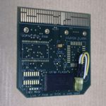
1M / 512K FLASH / 1M RAM PCB
updated 11th July 2013Contents
| Object | Detail | |
| Design Notes | Placing the components | |
| End Result | Post Production Errors | |
| Version 1.1 |
Parts List & History |
 Object
It has now been ten
years since the last Printed Circuit Board
(PCB) was designed to use the Intel Flash chip.
During that time we have seen Intel withdraw that chip and AMD bringing
out a version which we have used ever since. Spansion took over AMD but
they now have announced they have stopped manufacturing these range of
chips. Stocks of the previous flash chips and PCBs are running low, so
Rakewell bought the remaining stocks of 1M and 512K AMD Flash chips.All that remains is to design and build a PCB for these new flash chip before stocks run out.
When manufacturing a PCB, the cost is proportionate to
- the size of the card,
- the number of gold contacts,
- how many layers there are - a single layer is the cheapest but we want to aim for 2 layer.
- and how many are ordered at the same time.
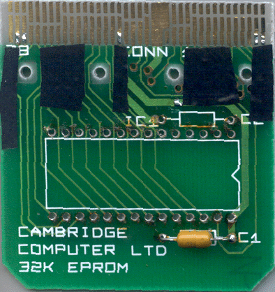
| When the Z88 was manufactured in
1988, a 32K EPROM chip (for example) took up half the space of the PCB
and had big pins to solder. Chip sizes now are a lot smaller and use Surface-mount technology. |
 |
Why not make one multifuctional card that share the
|
 |
It was decided that we could design a card to do FOUR functions.
|
Detail
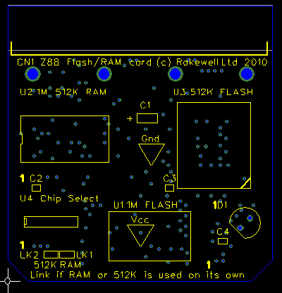
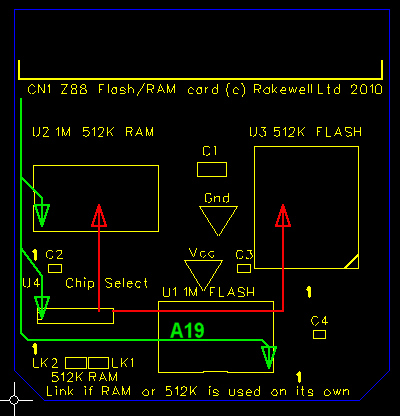
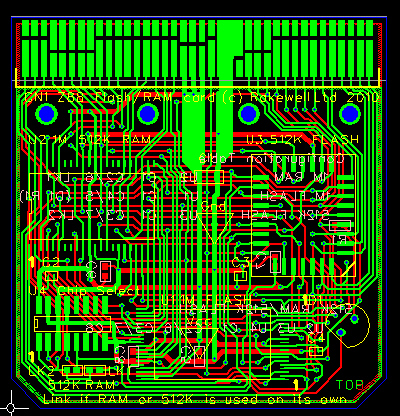
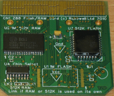
Circuit DiagramThis card gives maximum flexibility. There are 3 main memory chips, which gives 4 versions, 1M RAM, 1M FLASH. 512K FLASH / 512K RAM or 512K Flash.
U1 is tracked up to take 1M of FLASH. D1 and R1 are for the write LED that may be optionally fitted.
U2 is tracked up to take a 1M of RAM and is also used in the 512K RAM version
U3 is tracked up to take 512K of FLASH
U4 is used for the chip select logic in the 512K RAM / 512K Flash configuation.
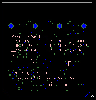
| Table | U1 | U2 | U3 | U4 | C1 | C2 / 6 | C3 / 7 | C4 / 5 | C8 | LK1 | LK2 | D1 | R1 |
| 1M RAM |  | | | | |||||||||
| 1M FLASH | | | | | | ||||||||
| 512K FLASH | | | | | |||||||||
| 512K RAM / 512K FLASH | | | | | | | |
Design Notes
I
thought I would share with you how I designed this card. The techniques
described all helped to 'untangle' tracks to the chips and use both
sides of the PCB to the best effect.Placing the components
| The
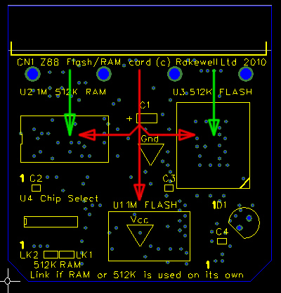
Z88 connector CN1 is fixed with power connections in the middle.
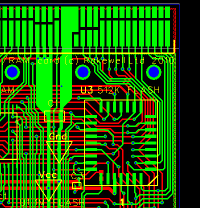
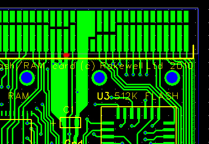
Power distribution is like a tree. These are shown in RED. All the other signals (shown in GREEN) are to the left and right of this and would need to be shared by U1, U2 and U3. The 1M Flash chip U1 all the pins required go straight to the Z88 connector CN1. It is placed centrally towards the back, allowing half the signals to go through the other two main chips (U2 RAM and U3 512K Flash). |
 |
 |
| Writing data to flash chips the program first addresses certain fixed registers.
This means that the address and data lines must go to the same
pins - e.g. D1 to D1, D2 to D2, A1 to A1, A2 to A2 and so on. The RAM U2 just reads and writes, so it doesn't care where the physical address or data 'location' is. The data (shown in RED) and address lines (shown in GREEN) on the chip could be changed to line up with the data and address lines on the Z88 connector CN1. |
 | The
512K Flash U3 lent itself to be placed on the right-hand side of the
board as the chip pinouts are simular to the old style DIL chips. I originally ran the red tracks towards the outside of the board underneath the green tracks, thinking that the inside of the chip would be crowded, but this was not to be the case. |
| The Chip Select U4 was placed at the bottom left because A19 was that side of the Z88 Connector. On reflection it wouldn't have mattered which side it went on as A19 also goes to U1 1M Flash. This is why the LED was placed on the right-hand side (after this picture was taken). The links select either the 1M RAM or the 512K Flash when the 512K RAM / 512K Flash and the Chip Select U4 is not used. |
 |
| Underneath the PCB the Configuration table was added. The decoupling capacitors were also placed here as well as on the component side. This was done just in case there was not enough room here for them. In the case of R1, if there is not enough space for it, it may have to be hard wired to the LED on the component side. |
 |
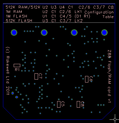
| In v1, the configuration table was moved up to the unused connector area for clarity. |
 |
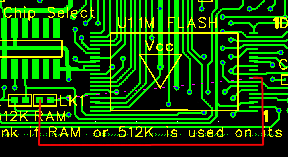
512K RAM / 512 Flash cardUsing the Test Points |
Testing the chips individually.
|
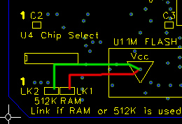 |
| This diagram shows the procedure used when deselecting either the 512K Flash (shown in GREEN) or the 1M RAM (shown in RED) after testing it. (Note the position of Vcc has been changed in v1). A small length of wire is used to connect Vcc to the right hand side pad of the device that needs to be deselected. |
1M Flash chip only |
 |
| The LED (D1) will come on when is actively erasing or programming. (This includes programming in the Erase Suspend mode.) If the output is high (LED off), the flash chip is ready to read array data (including during the Erase Suspend mode), or is in the standby mode. |
Function |
Default |
Notes |
Used |
Explanation |
| Copper to copper-fill clearance | 10 | 15 | is the clearance that FreePCB will create around traces or vias that pass through copper layers. | |
| Hole-edge to copper-fill clearance | 15 | 17 | is the clearance that will be created around drill holes. Please refer to Section 5.194: Drill Clearances for an important note about these clearances. | |
| Solder mask clearance | 8 | The pitch of the smallest chip is 1.27mm (50 mil) | 4 | the space that FreePCB will provide around pads in the solder masks. |
| Pilot hole diameter | 10 | 10 | the diameter of the pilot holes, if you selected them. Unable to change. | |
| Minimum silkscreen stroke width | 5 | Check | 5 | the minimum stroke width that FreePCB will use for the silkscreen layers, which is usually recommended by the board house. |
| Thermal relief line width | 10 | 10 | the width of the lines that will be used to connect pads or vias to copper fill areas using thermal reliefs. | |
| Board outline line width | 5 | 5 | the width of the board outline, if used. | |
| Annular ring width (pins) | 7 | 7 | ||
| Annular ring width (vias) | 5 | 5 |
Post Production Errors
As usual with a project this size there have been a few errors.Mechanical
The 45 degree corners need to be taken up by 2 mm to nearly where the track is.Electrical
| The Vpp needs to be disconnected |
 |
| The /CE needs to be connected to the 1M flash chip. |
 |
Version 1
- The Post Production errors have been corrected.
- The configuration table has been moved to the clear space on CN1.
- CN1 text moved to the centre of the connector.
- Link if RAM or 512K text made shorter.
- Rakewell's (c) & title of card moved to the other side.
- Capacitor pads have been increased in size.
Parts List & History
Farnell Parts List Now with pitch and size of chips
21/07/2009 Spansion are no longer manufacturing these chips - Rakewell buys up existing Farnell stock of 1M Flash.
13/11/2009 No more AMD 512K Flash chips from Farnel - considering AMIC - Programming change required.
01/12/2009 Rakewell locates part and buys up stock of AMD 512K Flash chips.
12/01/2010 Rakewell places order for the PCBs!
13/01/2010 Gunther points me to the places in the source code to add different Flash devices -
17/04/2010 Spansion manufactures 1M & 512K Flash chips (1M out of stock) AMIC Chips work.
04/12/2010 Low on stock of pre-production PCB. Work on Version 1 begins.
07/12/2010 Order placed for new batch of PCBs.
31/05/2013 Order placed for new batch of PCBs
10/07/2013 Problem with the Lyontek memory chip
Order |
Chip
|
Description |
pdf data sheet |
U1
|
AM29F080B-90ED 1Mx8 |
http:// |
|
|
U1 | AMD - | http://www.spansion.com/ |
1488943 |
U2
|
BS62LV8001EIP55 - |
http://www.farnell.com/ |
2253667 |
U2
|
LYONTEK - |
http://www.farnell.com/ |
1791222 |
U3 | SPANSION - | |
1791218 |
U3 |
SPANSION - |
http://www.farnell.com/ |
1565992 |
U3
|
AMIC - |
|
1085333 |
U4
|
74HC/HCT139 |
http://www.farnell.com/ |
1190107 |
C1
|
10uF Surface Mount |
http://www.farnell.com/ |
1288282 |
C2-8
|
0.1uF Case style: |
http://www.farnell.com/ |
1525564 |
D1 | SLR-56VR3F — ROHM | http://www.farnell.com/ |
1108764RL |
R1 | PCF0402-R-220R-B-T1. | http://www.farnell.com/ |
|
|
|||
8749493
|
FLASH 5V 4MB, | ||
|
|
Search for |

 |
|||||||
![[Click here to send e-mail for real-time pricing]](../images/click_prices_328.gif) |
|||||||
 | ![[ Top of Page ]](../images/top_of_page.gif) |

|
|||||
![[ Front Page ]](../images/home1.gif) |
![[ BBC BASIC ]](../images/bbc_basic.jpg) |
![[ Z88 Section ]](../images/z88.gif) |
![[ PC Section ]](../images/pc.gif) |
||||
| ©
[Rakewell Limited 1998 - Sep 2025] Rakewell 2025 - ? |
|||||||
|
|||||||
