
|
GENERAL |
|
Front Page |
|
 Pipedream |
|
|
Z88 |
|
Z88 |
|
Hardware |
|
 Spares Spares |
|
Software |
|
Shows |
|
Programmer's Section |
|
Quick Guide |
|
Reviews |
|
GDPR |
|
Help & FAQ |
|
Z88 2nd User Section |
|
|
EXTRA |
|
Site map |
|
| Feedback Help |
|
|
ARCHIVE SECTION |
|
|
GENERAL |
|
Adverts |
|
BBC BASIC |
|
Books |
|
Computer Fairs |
|
Flying Page |
|
PC |
|
|
NEWS |
|
Mailshot Promotions |
|
PC Newsletter |
|
 |
|
|
Z88 |
|
Z88 |
|
Hardware |
|
Software |
|
Saturday, 11-Apr-2026 10:50:22 BST
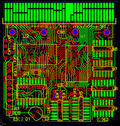
Z88 Projects
4M FLASH / 2M RAM PCB
updated 28th December 2009Object
This document explored using 4M Flash, this option is no longer possible.Our good friend Gunther has decided to retire from writing software for the Z88. I would like to take this opportunity to thank him for all the hard work he has done over the many years to get the Z88 to where it is now, with Flashstore, Eazylink, ROMupdate, updating ROMcombiner, OZ 4.2 - the list goes on and on!
From this point downwards, the document describes what we hoped to achieve before these larger chips became unavailable.
During the last year, new regulations regarding lead-free soldering has seen a large number of legacy components being removed from the lists and the AMD chip that we used, has moved to a smaller type package, a TSOP. A 4M version of the chip is also availabe, although we cannot access the 4M directly it is proposed that we use a register to select which of the 16M space you wish to use.
Three years ago a 1M static RAM was also released as a TSOP. Although I have a few 1M RAM packs left, they have always been expensive, because once they have gone there will be no more RAM packs left. These new RAM chips also consume far less power than the ones produced 20 years ago - this will have a positive effect on the battery life of the Z88.
The object of this document was to collect as many ideas as possible, and to incorporate them in this design as this could be the last time we design a card for the Z88. This is now approaching to be the final document, so if you have the time to check what has been written before I commit it to a PCB, it would be appreciated.
Detail
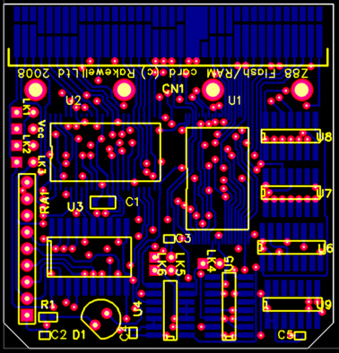
The main aim of this card is to give maximum flexibility. There are 2 main memory chips,
U1 is tracked up to take 8M of FLASH but we can only get 4M at present and
U2 is tracked up to take a 64M of RAM but we can only get a 2M RAM at present .
U3 is the REGISTER
U4 - U9 are decode and selection chips for the REGISTER.
U10 is the data bus level translator
RA1 are eight pull-up resistors
D1 is an LED that flashes when the REGISTER enable signal changes state.
Links are provided on the board to select each of the memory chips if they are used on their own in passive mode.
|
Configuration
|
LK 1 |
LK 2 |
LK 3 |
LK 4
|
LK 5 |
LK 6 |
RA1 1-2 |
| U5 IS FITTED | |||||||
| 1M RAM |  |
|
|||||
| 1M FLASH | |
|
|||||
| 512K
RAM / 512K FLASH |
|
|
|
|
|||
Larger versions are available when the REGISTER U3 is enabled and additional software is written. This will allow greater than 1M address space. The maximum amount of address space is 128M but the boad is only tracked to receive a flash chip up to 64M, once they make them. Mixed versions of flash and RAM are available from the following:-.
2M RAM
1M FLASH
2M FLASH THIS CHIP IS NOT GOING TO BE USED
4M FLASH
Circuit description
Click here for circuit diagram.There are three areas to consider.
Expanding the Memory Address space
The Z88 can address 1M of space. This space has been split into two 512K windows. The top half has access to write a value to the register and read and write to the top 512K of the flash chip. The bottom half will be pointing to a 512K section of the 128M address map that has been defined by the vaue that was written into the register beforehand.On start up, this may be a random selection. This means that you may be looking at 512K of RAM of Flash memory in the lower half. This should not matter as the program is run in the flash memory in the top half, which is always there.
Address lines A0 - A18, Data D0 - D7 and control lines (/OE, /WE) are standard and go to both the FLASH and RAM memory chips unmodified.
The expanded memory address lines AA19 - AA26 are generated by the REGISTER
The REGISTER
There are two things to consider for the register- Writing a value of data to the latch.
- Enabling the output to
use the data from the latch to generate the additional
addresses AA19 - AA26.
Writing a value of data into the latch
As the top half of the 1M Z88's address space is used for the flash chip, a method has to be used to be able to share the same address location for two different devices. It has been decided to use the very top byte of the address space to write to the register as well as having access to the flash card. This is acheived by the following method.To WRITE (any number) three times to address FFFFF in the Z88's external slot address space, followed by a WRITE to that location of the value that is required to be latched. For example,
- 00 would select the first 512K of RAM
- 03 would select the last 512K of the 2M RAM
- FC would select the first 512K of the 2M Flash
- FF
would select the last 512K of the Flash.
-
Note - This would not normally be used as this area is available direct from the top of the Z88's external slot address space, but it could be useful for testing the register.
Generating the /CLR or COUNT signal
The object of this chain is to generate a /CLR or COUNT output signal to reset a shift register, which is used as a counter.We want to write to a location at FFFF FF.
This is split into two selection processes.
A19 and /CE are dealt in the 2nd selection section which leaves
the decoding of the addresses and write line, A0 - A18 where are HIGH, and /WE is LOW are as follows:-
A1 & A2 are NANDed with U4.8 9 10
A3 - A18 are fully gated with 2 off, 8 bit NAND gates U7, U8.
These outputs go into the input of a 2-to-4 line decoder/demultiplexer
| U6a 2-to-4 line decoder/demultiplexer | ||||||
| INPUTS | OUTPUTS | |||||
| /G (U8.8) (L) | A (A1 & A2) (L) | B (U7.8) (L) | /Y0 | /Y1 | /Y2 | /Y3 |
| H | X | X | H | H | H | H |
| L | L | L | L | H | H | H |
| L | H | L | H | L | H | H |
| L | L | H | H | H | L | H |
| L | H | H | H | H | H | L |
A0 and /WE
These outputs go into the input of a 2-to-4 line decoder/demultiplexer, together with the output /Y0 from the previous 2-to-4 line decoder/demultiplexer giving the resulting output on /Y1.
| U6b 2-to-4 line decoder/demultiplexer | ||||||
| INPUTS | OUTPUTS | |||||
| /G (/Y0) (L) | A (A0 ) (H) | B (/WE) (L) | /Y0 | /Y1 (CLR) | /Y2 | /Y3 |
| H | X |
X | H | H | H | H |
| L | L | L | L | H | H | H |
| L | H | L | H | L | H | H |
| L | L | H | H | H | L | H |
| L | H | H | H | H | H | L |
This is the end of the A0 - A18 address and write decode.
2nd selection section
All the previous decoding is laying down the condition to count the register. Now we do the opposite, the condition to clear the counting of the register. The first thing you notice is rather than accepting /Y1 LOW, as we have in previous logic chains, we do the opposite this time and accept it when it is HIGH.The other two signals are for the clock and REGISTER select.
/OE - this drives the edge clock input and does the check everytime the Z88's signals are changing from being in a stable condition or not. (thank you Nigel Walker). It also gives the correct timing signal to write to the REGISTER.
/CE0 - if /CE0 is low, the RAM is being selected at the lower half of the memory, this is also the condition to clear the counting of the register, we are not at the top of the address space so the counter gets cleared. This gives us the signal for /CE and /A19 which would normally be used in a positive logic chain.
| U5b 2-to-4 line decoder/demultiplexer | ||||||
| INPUTS | OUTPUTS | |||||
| /G (/OE) (L) | A (CLR ) (H) | B (/CE0) (L) | /Y0 | /Y1 (/CLR) | /Y2 | /Y3 |
| H | X | X | H | H | H | H |
| L | L | L | L | H | H | H |
| L | H | L | H | L | H | H |
| L | L | H | H | H | L | H |
| L | H | H | H | H | H | L |
The /Y1 output is used as the
- /CLR input of the shift register U9.
This happens as soon as another address location is selected. If all the address bits are high, the /CLR input will be high and the following will happen.
Counting the number of writes
A shift register is used to count the number of clock cycles that the /CLR or COUNT signal has been in a high state for. If there is any change in the value of the /CLR input, the shift register resets and this operation would need to start again. As soon as the program addresses a different location, it will clear the shift register, and Q4 will then be LOW.The signal /OE (which is running all the time) is used as the clock and starts to shift the bit (the value of which has been set high on both pins A and B) first to QA, then QB, QC then when you write the fourth time, the bit will be at Q4. The normal state of this signal is LOW. This is the correct state so the output of Q4 is connected directly to the CK input of the latch. It should be noted that if further writes are made it will be the last value that will be latched.
Write to Latch Test LED
An LED is connected to the output signal for testing which can be removed in production versions (or left in as an option!).Enable the Register Latch
The REGISTER latch is an 8-bit positive edge triggered flip-flops. The data is transferred from the data bus to the Q outputs on positive going transitions of the CLOCK (CK) input. This value is enabled in the next section.Enabling the output
We
want to enable the output of the 8-bits from the REGISTER when the
lower half of the Z88's address space is selected. Fortunately, when
a high logic level is applied to the OUTPUT ENABLE (OE) input, all
outputs go to a high impedance state, regardless of what signals are
present at the other inputs and the state of the storage elements. When the REGISTER output is not selected, a resistor network RA1-8 2K2 block pulls up AA19 - AA26 on the output which ensures that the top of the Flash chip is selected in the extended address space when the Z88 is running in it's top half of memory.
Generating the Chip Select & Memory Map
The two address lines (A19 which is on the Z88 side & AA26 generated by the REGISTER) are used to select the following:-- RAM and NOT the REGISTER
- FLASH
PLCC32
Address A19 (when high) enables the FLASH, without any regard of the register's state.
Address AA26 (when high) also enables the FLASH
Address AA26 (when low) enables the RAM .
This combination gives the following Memory Map
| 1Mb
Address space, Z88 Card Connector |
"128M" Card map |
512K Register |
|||
| Top half is always the TOP 512K of 1M address space of card inserted in slot connector, and used to write to the REGISTER | 512K | <-- |
FLASH 4M, upper 512K This address space is always available. (reserved for OZ) |
512K | FF |
| Map 512K blocks here | 512K | <-- | FLASH 4M, lower 512K | 512K | FE |
| <-- | FLASH 3M | 512K | FD | ||
| <-- | 512K | FC | |||
| <-- | FLASH 2M | 512K | FB | ||
| <-- | 512K | FA | |||
| <-- | FLASH 1M | 512K | F9 | ||
| <-- | FLASH, first 512K | 512K | F8 | ||
| FLASH Not mapped | 80 - F7 | ||||
 |
|||||
| <-- | 64M, END OF RAM | 512K | 7F | ||
| <-- | 512K | 7E | |||
| <-- | ... | ... | ... | ||
| <-- | 2M | 512K | 03 | ||
| <-- | 512K | 02 | |||
| <-- | 1M, RAM (upper) | 512K | 01 | ||
| <-- | 512K, RAM (lower) | 512K | 00 | ||
Decoding the addresses
A 2-to-4 line decoder/demultiplexer is used to generate the CE signals for the memory from /CE, A19 and AA26 as follows:-
| U5a 2-to-4 line decoder/demultiplexer | ||||||
| INPUTS | OUTPUTS | |||||
| /G (/CE) | A (A19) | B (AA26) | /Y0 | /Y1 | /Y2 | /Y3 |
| H | X | X | H | H | H | H |
| L | L | L | L | H | H | H |
| L | H | L | H | L | H | H |
| L | L | H | H | H | L | H |
| L | H | H | H | H | H | L |
| RAM | FLASH | NOT USED | ||||
Selecting the RAM and REGISTER /Y0
We have two sizes of RAM chips, 1M or 2M they both use the same address and pad space when AA26 is low.
Only one of them are used at any one time as they both use the same /CE 0 signal to select them..
This method will give multiple images of the RAM space, but the Z88 software will find the RAM boundaries itself, just like it does with smaller RAM cards, like the 32K.
The REGISTER is also selected with this signal as it is in the negative part of the selection change i.e. when the RAM is selected, the REGISTER isn't selected - see the REGISTER for a better explanation of this.Selecting the Flash chip
There is only one flash chip irrespective of its size. This gets selected when either the Z88's A19 is high or AA26 is high. This is a OR gate and is generated as follows:-
/Y1 is NANDed with /Y2 THEN inverted.| U4 456 INVERTOR | |||
| INPUT | OUTPUT | ||
| U4 123 NAND GATE | |||
| INPUTS | OUTPUT | ||
| /Y1 (/CE1) | /Y2 (/CE2) | Y1 /Y2 | |
| H | H |
L |
H |
| L | H |
H |
L |
| H | L |
H |
L |
| L | L | H | L |
| U4 11 12 13 NAND GATE | ||
| INPUTS | OUTPUT | |
| /Y1 (/CE1) | /Y2 (/OE) | |
| H | H |
L |
| L | H |
H |
| H | L |
H |
| L | L | H |
List of points and answers
Here are the points made before, my comments are in bold afterwards.1M/4M Flash Chip
The 1M Flash chip uses the same pad layout as the larger sizes, so all the address lines have been tracked including some that go to 'no connection' pins (in the hope that they will be the correct pins for larger chips).2M/1M RAM Chip
This is the same as the Flash chip, see above.512K Flash Chip
This chip has been considered but as the price is only a few pence cheaper than the 1M, there is no space. The 1M size can be used instead and ignoring the other half. There is no 512K Flash chip.Points arising
512K Flash card and 512K RAM - No longer an option
Thierry has pointed out that if a 512K Flash card and 512K RAM could be accommodated, then the new version of OZ could run in that. I am assuming that the Flash area would be at the top i.e. A19 high and the 512K RAM would be at the lower end A19 low. Gunther has confirmed that this combination works with OZ2.2 using the emulator.31/03/2009
Gunther used the 512K Flash chip for his test. This chip is not supported in the TSOP package type. Further research shows that the 512K Flash chip is no longer going to be manufactured which means that this configuration will not work at present. It has been decided not to offer this configuration and just press on with the software for the larger sizes.
If you want a 512K RAM and FLASH, a 1M FLASH and RAM with U5 should be fitted. This will not work with the current software as when the 1M Flash chip is identified it assumes that the complete area is available (which it is normally). The additional space in both the RAM and FLASH chips will be discarded until the register software is written. There are additional links on the board to allow for this configuration.
Parts List
Farnell Parts List Now with pitch and size of chips
21/07/2009 Spansion are no longer manufacturing these chips - Rakewell buys up existing 1M Flash chips Farnell stock
| Order Code |
Chip No |
Description |
PDF Data Sheet |
|---|---|---|---|
120-1511 |
U1 |
AM29F080B-90ED |
http:// |
1607574
|
U1 |
AM29F080B-90EF IC, |
|
MX29F016 2M x 8 |
http:// |
||
120-1503 |
U1 |
AM29F032B-90ED 4Mx8 |
http:// |
869-8201 |
U2 |
BS62LV8001 1Mx8 RAM |
http:// |
| U2 |
BS62LV8001EIP55 |
http:// |
|
1488943
|
U2 |
BS62LV8001EIP55 |
http:// |
1271840 |
U2 |
BS62LV8001 1Mx8 RAM |
http:// |
| U2 |
BS62LV1600EIP55 -
|
http:// |
|
9591737 |
U4 |
QUADRUPLE 2-INPUT |
http:// |
1085333 |
U5 U6 |
74HC/HCT139 Dual
|
http:// |
1013977 |
U3 |
74HC CMOS, SMD, |
http:// |
1085303 |
U7 U8 |
74HCT30D CMOS LOGIC |
http:// |
1085337 |
U9 |
74HC164; 74HCT164 |
http:// |
9356916 |
RA1 |
4600X Series Thick |
http:// |
1190107 |
C1 |
10uF Surface Mount |
http:// |
1288282 |
C2 - C5 |
0.1uF Case style: |
http:// |
1525564 |
D1 |
SLR-56VR3F — ROHM — |
http:// |
1108764RL |
R1 |
PCF0402-R-220R-B-T1 |
http:// |
1201488
|
U3 |
4 Megabit (512 K x |
http:// |
1201510
|
ATMEL - AT49BV322D |
http:// |
|
9453083
|
TRANSLATOR, SMD, |
http:// |
38 1
Connection list
Slot |
Desc |
BS62LV8001 |
AM29F080B |
BS62LV4006 |
AM29F040B |
1 |
A16 |
21 |
4 |
2 |
2 |
2 |
A15 |
22 |
5 |
31
|
3 |
3 |
A12 |
25 |
8 |
4 |
4 |
4 |
A7 |
42 |
17 |
5 |
5 |
5 |
A6 |
43 |
18 |
6 |
6 |
6 |
A5 |
44 |
19 |
7 |
7 |
7 |
A4 |
1 |
20 |
8 |
8 |
8 |
A3 |
2 |
21 |
9 |
9 |
9 |
A2 |
3 |
22 |
10 |
10 |
10 |
A1 |
4 |
23 |
11 |
11 |
11 |
A0 |
5 |
24 |
12 |
12 |
12 |
D0 |
9 |
25 |
13 |
13 |
13 |
D1 |
10 |
26 |
14 |
14 |
14 |
D2 |
13 |
27 |
15 |
15 |
15 |
SNSL |
- | - |
- |
- |
16 |
GND |
12 |
29 |
16 |
16 |
17 |
GND |
34 |
30 |
- |
- |
18 |
A14 |
23 |
6 |
3
|
29 |
19 |
VCC |
40 CE2 |
31 |
- |
- |
20 |
VCC |
11 |
10 |
32 |
32 |
21 |
VCC |
33 |
12 RESET |
- |
- |
22 |
WEL |
17 |
38 |
29
|
31 |
23 |
A13 |
24 |
7 |
28 |
28 |
24 |
A8 |
39 |
16 |
27 |
27 |
25 |
A9 |
28 |
15 |
26 |
26 |
26 |
A11 |
26 |
13 |
25 |
25 |
27 |
POE |
- | - |
- |
- |
28 |
ROE |
41 OE# |
37 OE# |
24 OE# |
24 |
29 |
A10 |
27 |
14 |
23 |
23 |
30 |
SE1 |
6 |
9 |
22 |
22 |
31 |
D7 |
36 |
35 |
21 |
21 |
32 |
D6 |
35 |
34 |
20 |
20 |
33 |
D3 |
14 |
28 |
17 |
17 |
34 |
D4 |
31 |
32 |
18 |
18 |
35 |
D5 |
32 |
33 |
19 |
19 |
36 |
A17 |
20 |
3 |
30 |
30 |
37 |
A18 |
19 |
2 |
1 |
1 |
38 |
A19 |
18 |
1 |
- |
- |
- |
- | - |
36 RY/BY 39 SW 40 SW |
- |
- |
Netlist
$PACKAGES
! 10uF; C1
! 0.1uF; C2
! 0.1uF; C3
! 0.1uF; C4
! 0.1uF; C5
! CN-38P; CN1
! LED; D1
! /CE RAM; LK1
! /CE FLASH; LK2
! A19 AA19; LK3
! NO REG1; LK4
! NO REG2; LK5
! NO REG3; LK6
! 220R; R1
! 8 x 2K2; RA1
! AM29F032B; U1
! BS62LV1600; U2
! 74374; U3
! 7400; U4
! 74139; U5
! 74139; U6
! 7430; U7
! 7430; U8
! 74HC164; U9
! Vcc; Vcc0
$NETS
A16; CN1.1 U1.4 U2.44 U7.3
A15; CN1.2 U1.5 U2.42 U7.4
A12; CN1.3 U1.8 U2.4 U7.12
A7; CN1.4 U1.17 U2.5 U8.3
A6; CN1.5 U1.18 U2.43 U8.4
A5; CN1.6 U1.19 U2.19 U8.11
A4; CN1.7 U1.20 U2.20 U8.12
A3; CN1.8 U1.21 U2.21 U8.1
A2; CN1.9 U1.22 U2.22 U4.10
A1; CN1.10 U1.23 U2.39 U4.9
A0; CN1.11 U1.24 U2.24
D0; CN1.12 U1.25 U2.9 U3.3
D1; CN1.13 U1.26 U2.10 U3.4
D2; CN1.14 U1.27 U2.13 U3.7
GND; C1.2 C2.2 C3.2 C4.2 C5.1 ,
CN1.16 CN1.17 LK5.2 LK6.2 R1.1 ,
U1.29 U1.30 U2.12 U2.34 U3.10 ,
U4.12 U4.13 U4.7 U5.8 U6.8 ,
U7.7 U8.7 U9.7
A14; CN1.18 U1.6 U2.23 U7.6
VCC; C1.1 C2.1 C3.1 C4.1 C5.2 ,
CN1.19 CN1.20 CN1.21 RA1.1 U1.10 ,
U1.12 U1.31 U2.11 U2.33 U2.40 ,
U3.20 U4.14 U5.16 U6.16 U7.14 ,
U8.14 U9.1 U9.14 U9.2 Vcc.1
/WE; CN1.22 U1.38 U2.17 U6.13
A13; CN1.23 U1.7 U2.26 U7.5
A8; CN1.24 U1.16 U2.27 U8.2
A9; CN1.25 U1.15 U2.28 U8.5
A11; CN1.26 U1.13 U2.25 U7.11
/OE; CN1.28 U1.37 U2.41 U5.15 U9.8
A10; CN1.29 U1.14 U2.3 U8.6
/CE; CN1.30 LK1.2 LK2.2 U5.1
D7; CN1.31 U1.35 U2.14 U3.13
D6; CN1.32 U1.34 U2.31 U3.14
D3; CN1.33 U1.28 U2.32 U3.8
D4; CN1.34 U1.32 U2.35 U3.18
D5; CN1.35 U1.33 U2.36 U3.17
A17; CN1.36 U1.3 U2.2 U7.2
A18; CN1.37 U1.2 U2.1 U7.1
A19; CN1.38 LK3.1 U3.1 U5.3
AA19; LK3.2 RA1.2 U1.1 U2.18 U3.2
AA20; RA1.3 U1.40 U2.16 U3.5
AA21; RA1.4 U1.39 U2.15 U3.6
AA22; RA1.5 U1.11 U2.29 U3.9
AA23; RA1.6 U2.30 U3.19
AA24; RA1.7 U2.7 U3.16
AA26; LK5.1 RA1.8 U3.12 U5.2
AA25; RA1.9 U2.8 U3.15
/CE3; LK2.1 LK4.1 U1.9 U4.6
/CE0; LK1.1 U2.6 U5.13 U5.4
N00000; U4.8 U6.2
CLR; LK6.1 U5.14 U6.11
N00001; U5.11 U9.9
/CE1; LK4.2 U4.1 U5.5
/CE2; U4.2 U5.6
N00002; U6.3 U7.8
N00003; U6.1 U8.8
N00004; U6.15 U6.4
RR; D1.1 U3.11 U9.6
N00005; U4.3 U4.4 U4.5
N00006; D1.2 R1.2
$END
 |
|||||||
![[Click here to send e-mail for real-time pricing]](../images/click_prices_328.gif) |
|||||||
 | ![[ Top of Page ]](../images/top_of_page.gif) |

|
|||||
![[ Front Page ]](../images/home1.gif) |
![[ BBC BASIC ]](../images/bbc_basic.jpg) |
![[ Z88 Section ]](../images/z88.gif) |
![[ PC Section ]](../images/pc.gif) |
||||
| ©
[Rakewell Limited 1998 - Sep 2025] Rakewell 2025 - ? |
|||||||
|
|||||||