
|
GENERAL |
|
Front Page |
|
 Pipedream |
|
|
Z88 |
|
Z88 |
|
Hardware |
|
 Spares Spares |
|
Software |
|
Shows |
|
Programmer's Section |
|
Quick Guide |
|
Reviews |
|
GDPR |
|
Help & FAQ |
|
Z88 2nd User Section |
|
|
EXTRA |
|
Site map |
|
| Feedback Help |
|
|
ARCHIVE SECTION |
|
|
GENERAL |
|
Adverts |
|
BBC BASIC |
|
Books |
|
Computer Fairs |
|
Flying Page |
|
PC |
|
|
NEWS |
|
Mailshot Promotions |
|
PC Newsletter |
|
 |
|
|
Z88 |
|
Z88 |
|
Hardware |
|
Software |
|
Saturday, 11-Apr-2026 10:48:08 BST
Z88 Projects
512K FLASH Adapter
Although I have written this up to show you what I did, I will never do this project again as it damaged the connector on the Z88.
Dual Powered Willem Universal EPROM Programmer+27C256 programmers that can be used with the PC are not a lot of money and can be obtained on Ebay for around £20 which is around the component cost of this project.
Object
In order to use a 512K Flash chip (AM29F040B) in the Z88 to store the Operating System OZ it is necessary to blow the image to the chip to start with. This is done by producing an adapter that plugs into the Z88's card slot, so that the Flash chip can be blown.After this procedure, the chip and adapter is removed and the chip is then placed into a modified Z88 to run. The adapter is only required once because once an Operating System is running in the Z88, the flash chip may be updated internally.
There is not enough room in the Z88 card pack to fit an IC socket, so a flying ribbon cable is used allowing the chip and socket to be both outside the case and Z88.
If a 512K Flash card is required, then the chip may be soldered inside the Z88 pack using the wiring diagram as described.
Method
Although soldering ribbon cable to holes and sockets is possible, this method uses standard IDC connectors to cut the soldering down to a minimum, ensuring a strong mechanical construction as well.Tools required
Vice, G clamp or IDC toolSoldering iron
solder
De-soldering pump
Hacksaw
File
Small screwdriver
Pair of scissors
continununity meter
This list makes up one adapter.
Parts List
Z88 Parts List
Qty Order Code Description
1 32K EPROM Pack
Farnell Parts List
Qty Order Code Description
1 109-7041 SOCKET, IDC NO S/RELIEF 34WAY; RoHS Comp
1 101-2214 CABLE ASSY, RIBBON 34 WAY 20 CM; RoHS Co
 1      110-6722      PLUG, IDC DIP 28WAY; Ways, number of:28

 1      102-3062      IC SOCKET, DIL 32 WAY PK12
1 120-1510 IC, FLASH 4MB; RoHS Compliant:NO; Memory
Odds & Sods
1 Insulating tape or paper
Preparation
This is not an easy project. When I started it took me five hours to build one.With a small screwdriver carefully break open the 32K EPROM pack. The label comes off first showing you the 4 posts that are holding the two halves together. The small thin plastic cover is next, followed by the PCB. Start at one end and gently lever the PCB away from the rest of the plastic case. If you hear a sharp click, this may mean you have broken the post, which is not desirable.
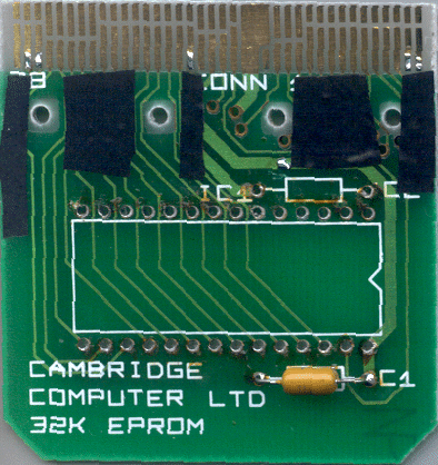
PCB Preparation
Once the PCB is removed, you can unsolder the 32K EPROM chip IC1 and the resistor C2 from the board using a soldering iron and de-soldering tool. I found you needed to cut the 32K EPROM away from its pins first and then unsoder each pin. Soldering it and then unsoldering the pin works best as the solder is pretty old and doesn't move easily. Use small strips of insulating tape to stop the bare wires that are used shorting with the tracks underneath, missing the 4 holes.Tin the following edge connector numbers, with just a tiny bit of solder, leave all the gold you can spare where it is.
1
2
22
36
37
Locate the horizontal track with Vcc and scrape and tin it next to the 2nd hole from the right.
Cable Preperation
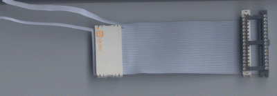
Slide the SOCKET, IDC NO S/RELIEF 34WAY onto the cable making sure that the socket and the key (the bump along one edge) is the same way round as the fitted socket already on the cable (to the right see picture).
Plug in the IC SOCKET, DIL 32 WAY, using the outside pins of the two sockets to connect to the pins of the IC socket just to get the correct spacing. When you have the spacing of the two SOCKET, IDC NO S/RELIEF 34WAY correct, use the vice to squeeze the connector together without the IC SOCKET, DIL 32 WAY being there otherwise you will damage it and the connector will twist..
The IC SOCKET, DIL 32 WAY is placed with pin 1 at the top, with the extra 2 holes above it, the cable leaves the socket on the left-hand side.
----------- x x x x
1 o o
o o
cable to
Z88 card
That is the 512K Flash Chip end done, now for the Z88 Card end.
Z88 Card
Now here is where it gets a bit complicated. We are using 34 way cable to connect a 32 pin chip to the bottom 26 pins of a 28 pin chip. Here is the breakdown.Top 2 SPARE
Next 4 to be soldered
Next 2 to be soldered but have gone through the PLUG, IDC DIP 28WAY unused
Rest 26 use PLUG, IDC DIP 28WAY; Ways, number of:28
Split the cable 2 wires down from the pin 1 end completely to the first IDC connector and cut these away. They are not used.
Split the next 4 wires 90 mm wires down from the Pin 1 end which should leave you with 28 ways.
Fit the PLUG, IDC DIP 28WAY; to the other end of the ribbon cable, at the start where the split is, the cable coming in from the right, pins downwards . Use the vice again, I used a couple of those IDC connctors to protect the pins whilst compressing it.
Split the next 2 wires down to the PLUG, IDC DIP 28WAY and cut off the two pins (1 and 28) underneath.
With a meter, check that there is a connection between the pins of the PLUG, IDC DIP 28WAY and the SOCKET, IDC NO S/RELIEF 34WAY end. Checking the corner pins on the plug is a good guide because the bottom two pins should be where you would expect them to be, but the top two start 4 sockets down. If you don't get this, check that you have cut those two pins off.
Cut the remaining wires off close to the PLUG, IDC DIP 28WAY.
Joining them up together
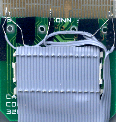
Solder the PLUG, IDC DIP 28WAY into the space of the removed 32K EPROM chip. SSolder just two diagonal pins first and make sure that the plug is as close to the PCB as possible. Then cut all the pins that are slightly sticking up from the PCB. There is no room for these. Then solder all the pins.Starting with the power wire, Vcc which is the first wire nearest to the top is soldered to the horizontal track tinned earlier. I split the single wire just enough to reach that pad. That way you keep all the wires together.
Make long tails on the following wires now as they need to go underneath the plastic divider. They need to be bare as soon as they reach those four round holes down to the edge connector.
The next wire goes to edge connector 37 which is nearly at the far end.
Edge connector 22 is next followed by 1.
You should be now on the two wires that go through the PLUG, IDC DIP 28WAY which go to 36 and 2.
With a small screwdriver you need to remove the 'lid' on the PLUG, IDC DIP 28WAY. There is no hieght to leave this on. With the wire cutters, cut off the two lid locators on the left and right hand side. There is no hieght for these either.
The cable leaving the card needs to be folded on itself at the 'spare wire end' or the pin 1 end as it won't go out of the front of the card housing correctly.
Before putting it back into the case - check all the connections for continuety and shorts. It's easier to do these now than later.
38 1
Slot RAM/ROM RAM/ROM Eprom Pins for
pins Signals 512K
                FLASH
              AM29F040B
1       A16     2
2       A15     3
3       A12     4
4       A7      5
5       A6      6
6       A5      7
7       A4      8
8       A3      9
9       A2      10
10      A1      11
11      A0      12
12      D0      13
13      D1      14
14      D2      15
15      SNSL     -
16      GND     16
17      GND     16
18      A14     29
19      VCC     -
20      VCC     32
21      VCC     -
22      WEL     31
23      A13     28
24      A8      27
25      A9      26
26      A11     25
27      POE     -
28      ROE     24
29      A10     23
30      SE1     22
31      D7      21
32      D6      20
33      D3      17
34      D4      18
35      D5      19
36      A17     30
37      A18     1
38      A19     -
 1       SPARE +--------------------+ SPARE
 2    37   A18 |1       +--+      32| VCC  +--20
      1    A16 |2                 31| WE   |  22
      2    A15 |3   1 VPP VCC 28  30| A17  +  36
           A12 |4   2 X     X 27  29| A14
           A7  |5   3 X     X 26  28| A13
           A6  |6   4 X     X 25  27| A8
           A5  |7   5 X     X 24  26| A9
           A4  |8   6 X     X 23  25| A11
           A3  |9   7 X     X 22  24| OE
           A2  |10  8 X     X 21  23| A10
22         A1  |11  9 X     X 20  22| CE
           A0  |12 10 X     X 19  21| D7
           D0  |13 11 X     X 18  20| D6
36         D1  |14 12 X     X 17  19| D5
37         D2  |15 13 X     X 16  18| D4
38         VSS |16 14 X     X 15  17| D3
               +--------------------+
Just using a 512K chip
If you just want to use the 512K Flash chip as an external card, you just need to bend up the 6 pins, solder the rest into the PCB and then connect the other 6 connections as described above.Mechanical details
Before putting it together again, do the following:-
- Make a slot for the ribbon cable to leave the Z88 card case. Use the hacksaw to cut down and then file the rest of it down.
- The extra wires at the top need
to be folded underneath so that they can go through the middle of the
card without hitting the edge where the plastic pins go through for the
cover.
- Check all the electrical connections before inserting any chips for short circuits and continuity
Z88 details
The ROM chip socket needs the following changes:-
Five changes Swap A16 & ROE, add A17, A18 & WE - Pin numbers are the memory card pin numbers.
               +--------------------+
      37   A18 |1 VCC   +--+  VCC 32| VCC     20
      1    A16 |2 ROE <--+    VCC 31| WE      22
      2    A15 |3 A15    |    VCC 30| A17     36
           A12 |4        |        29| A14
           A7  |5        |        28| A13
           A6  |6        |        27| A8
           A5  |7        |        26| A9
           A4  |8        |        25| A11
           A3  |9        +-->A16  24| ROE
           A2  |10                23| A10
           A1  |11                22| CE
           A0  |12                21| D7
           D0  |13                20| D6
           D1  |14                19| D5
           D2  |15                18| D4
           VSS |16                17| D3
               +--------------------+

 |
|||||||
![[Click here to send e-mail for real-time pricing]](../images/click_prices_328.gif) |
|||||||
 | ![[ Top of Page ]](../images/top_of_page.gif) |

|
|||||
![[ Front Page ]](../images/home1.gif) |
![[ BBC BASIC ]](../images/bbc_basic.jpg) |
![[ Z88 Section ]](../images/z88.gif) |
![[ PC Section ]](../images/pc.gif) |
||||
| ©
[Rakewell Limited 1998 - Sep 2025] Rakewell 2025 - ? |
|||||||
|
|||||||